The term’ optic’ is related to light, and when signals travel over the light waves for communication, it is known as optical networking. In optical networks, fiber optic cables are used as a communication medium. They have revolutionized communication by achieving a data speed of several terabits per second. Optical networking is used in a wide variety of applications, such as video streaming, cloud computing, and virtual reality. Optical networking is used for long-distance communication, and it transmits large amounts of data quickly over long distances with minimal loss of signal quality. Its most crucial component is the fiber optic cables through which the signals travel. A vast and sophisticated network of these cables has been laid to carry the signals uninterrupted over long distances. Another component revolutionizing communication through optical networking is silicon wafers. These are thin, circular silicon discs. They are used in producing electronic components, particularly integrated circuits (ICs). Integrated circuits comprise a complex network of transistors, capacitors, and other components interconnected on a silicon base, also called a silicon wafer. Silicon wafers are the core of making memory chips, microprocessors and many other semiconductor devices. They are also at the core of high-speed optical communication networks. When these silicon wafers are modified to include certain patterns on their surface, they are called patterned silicon wafers. The patterning allows the creation of specific optical components with high accuracy and precision.
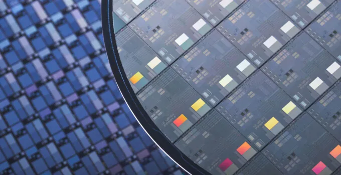
Source: eetasia.com
Page Contents
Meaning Of Patterning
Patterning means creating a certain pattern on the silicon wafer. This pattern is created by fabricating various optical and electronic components on the wafer, resulting in a photonic integrated circuit (PIC). Various layouts of these components lead to various patterns and functionalities of PICs.
Role Of Patterning
Patterning makes it possible to create certain patterns or structures on the surface of the wafer. These patterns are capable of creating PICs with varied functionalities. PICs can be used in high-speed optical communication networks and optical sensing systems. Some common components with silicon wafers include optical modulators, transceivers and interconnects.
Making Silicon Wafers
The process of making silicon wafers begins with the purification of raw silicon. After purification, silicon is melted and formed into a single crystal, which is then sliced into thin slices, hence the name wafers. This slicing is generally done using a diamond saw. The wafers are then polished to remove any imperfections and are then treated with various chemicals to create the desired electrical properties.

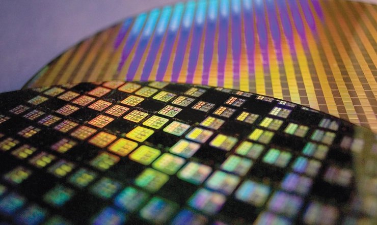
Source: linkedin.com
Ways To Get Patterning Done
There are various technologies for performing patterning. A few are discussed below:
Photolithography
In this technology, light is used to transfer a pattern onto a silicon wafer and create complex structures and features. A mold, also referred to as a mask, is used to transfer the pattern on the wafer. First, the wafer is coated with a photoresist material. Then the mask is transferred over it. Now when they are exposed to light, a chemical reaction occurs, leaving behind a patterned layer of photoresist on the wafer.
Chemical Vapor Deposition (CVD)
In this technology, a mask of a thin film is deposited on the silicon wafer by introducing gaseous reactants into a reaction chamber and allowing the reactants to undergo a chemical reaction on the wafer surface.
Electron Beam Lithography
In this technology, a focused beam of electrons is used to create a pattern on the wafer. The focused beam can create minute features with high precision, making it suitable for advanced patterning.
Nanoimprint Lithography
This technology is very similar to photolithography. In it, a thin layer of resist material, like a UV-curable polymer, is applied to the wafer using spin-coating. Then a mask is used to create a pattern under force and pressure in a controlled manner. It is a simpler and faster technology.

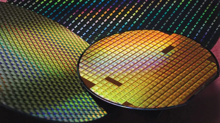
Source: techpowerup.com
Advantages Of Patterned Wafers
Highly Precise And Accurate
The patterning of the silicon wafer helps create complex optical structures with high precision and accuracy. Very specific optical components, such as waveguides, filters, and modulators, can be created and integrated to make complex PICs. These components lead to successful optical networking.
Provide High-speed
Speed is an important aspect of any communication network. Gone are the days when people had to wait for buffering. If the components are not able to provide high speed, they are considered lacking. Silicon makes an attractive base material for high-speed devices due to its excellent electronic and optical properties. It has high electron mobility, which allows for fast switching speeds in electronic devices. Additionally, silicon has a high refractive index, making it a useful material for fabrication.
Low Power Consumption
Patterned wafers themselves may not be responsible for working on low-power, but they do provide a stable and well-controlled platform for low-power consumption components to be fabricated on them.

Source: gep.com
Compatibility
Patterning techniques used on silicon wafers are compatible with existing semiconductor fabrication techniques. It means manufacturing patterned silicon wafers did not require a significant infrastructure overhaul. The fabrication and patterning are compatible with existing techniques.
Economical
The patterning process can be undertaken using high-volume, low-cost manufacturing techniques, making the production of complex devices more cost-effective.
Small Size
Patterning allows for the creation of very small device features, which can enable the miniaturization of electronic and photonic devices. Also, this small-size integration leads to improved overall system performance and reduced need for separate components. This is particularly important in optical networking, where minute optical sensors are used.
Source: tomshardware.com
Conclusion
The usage of patterned silicon wafers in optical networking has brought a revolution in communication. The patterning of silicon wafers makes complex and precise structures to be fabricated on the wafers. It has led to the overall improved performance of the devices used in optical networking. This is particularly important as high precision and accuracy are necessary for achieving high-speed operations in optical networks. In the future, even higher speeds and better performance are expected with the newer technologies being introduced in optical networking.


